Personal computing discussed

Moderators: renee, Flying Fox, morphine

 
chuckula
Minister of Gerbil Affairs
Topic Author
Posts: 2109
Joined: Wed Jan 23, 2008 9:18 pm
Location: Probably where I don't belong.

Bad Intel Docs & Skylake X die size estimate

Thu Jun 01, 2017 9:45 pm

EDIT: If you want the TL;DR version, Gamer's Nexus took a ruler to the die (a luxury I don't have unfortunately)

The life blood of any engineer: sweet sweet documentation.

Unless it's just bizarrely wrong. And that's the case that I dug up on Intel's website with a link to the Skylake X series data sheet (volume 1, in volume 2 I hear they kill Bill).

This document has a juicy sounding title but when you read it you rapidly realize that while it says "Skylake X" a whole bunch of the content is clearly copy-n-pasted directly from Broadwell's datasheet without updates while simultaneously sprinkling in mentions of Skylake X.... BAD INTEL! NO DOCUMENTATION AWARD FOR YOU! Maybe they were hacked, or maybe they posted that as a joke.

Anyhoo, the reason I cared was that I wanted to get the dimensions of an LGA-2066 package so I could get my first estimate of the small (12 core) Skylake X die size. I'm assuming (always a dangerous thing) that the information in section 1.6 at the top of page 13 is correct:
The processor socket type is noted as LGA2066. The processor package is a 52.5 x 45 mm FC-LGA package.


If you are wondering, that's suspiciously similar (as in exactly the same) to LGA-2011. Not impossible considering 55 contacts don't take up that much space and LGA-2066 is clearly not radically different in size from LGA-2011. However, it's a caveat that if those numbers are wrong it will impact the accuracy of the analysis.

Phase 2: get a halfway decent picture of a delidded Skylake X with the package.

This one comes to use courtesy of HardwareLux.de concerning a guy named der8auer who makes delidding kits.

Reproduced here:
Image

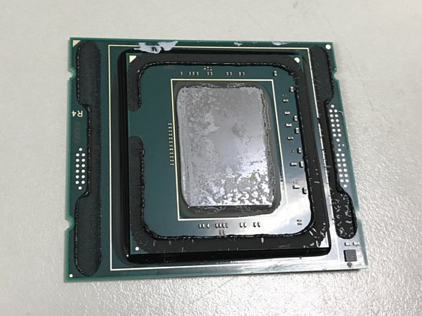
If anybody's wondering, that's regular thermal paste. For my purposes the only problem I have is they didn't clean it off, but we'll see what we can do with estimating a die size. Furthermore, this image is at far from a perfect plan view so take this estimate as a first attempt with some error wiggle room. Note: The upside-down "R4" is on the short edge (45 mm) of the package (other photos with the IHS still on show that more clearly).

And now for my pixel-counting magic I get:

Chip width (narrow side of chip, long edge (52.5 mm) of package): 14.57 mm. (Note: The thermal paste introduces a big margin for error here, I gauged along the very bottom edge where you can just see a squared corner).

Chip height (long side of chip, short edge (45 mm) of package): 22.44 mm.

Total area: 327 mm^2.

This is a 12 core die Edit: Turns out it's a 10 core die, the original information stating that it's 12 was inaccurate, take the rest with that grain of salt. Its predecessor, the 10 core Broadwell-E die, weighs in at 246 mm^2. While not a perfect metric because there's a lot more to a chip than just the core [Edit: for anybody not reading this carefully, I am NOT saying each core is actually the size listed below], a straight measure of square millimeters per core gives us:
Broadwell: 24.6 mm^2 per core
Skylake: 27.25 mm^2 per core.

So Skylake X is on a "per core" basis about 11% bigger than its predecessor. At least if this estimate is even in the ballpark. I look forward to hopefully having Intel give us real numbers soon.
Last edited by chuckula on Tue Sep 05, 2017 3:13 pm, edited 2 times in total.
4770K @ 4.7 GHz; 32GB DDR3-2133; Officially RX-560... that's right AMD you shills!; 512GB 840 Pro (2x); Fractal Define XL-R2; NZXT Kraken-X60
--Many thanks to the TR Forum for advice in getting it built.
 
Shobai
Gerbil First Class
Posts: 165
Joined: Sat Sep 03, 2005 1:18 am

Re: Bad Intel Docs & Skylake X die size estimate

Thu Jun 01, 2017 11:16 pm

The Gamer's Nexus article I posted over on the frontpage article has a more square-on shot, if you wanted to try to adjust that for keystone? I can't imagine the measurements will be much different than what you came up with here, though.
 
Topinio
Gerbil Jedi
Posts: 1839
Joined: Mon Jan 12, 2015 9:28 am
Location: London

Re: Bad Intel Docs & Skylake X die size estimate

Fri Jun 02, 2017 1:27 am

Oh, Intel docs ... so, so bad :( Why, for the love of $DEITY, is there no publication of the Turbo Boost per-core bins and the AVX boost frequencies? I want to know the peak GFLOPS...
Desktop: 750W Snow Silent, X11SAT-F, E3-1270 v5, 32GB ECC, RX 5700 XT, 500GB P1 + 250GB BX100 + 250GB BX100 + 4TB 7E8, XL2730Z + L22e-20
HTPC: X-650, DH67GD, i5-2500K, 4GB, GT 1030, 250GB MX500 + 1.5TB ST1500DL003, KD-43XH9196 + KA220HQ
Laptop: MBP15,2
 
chuckula
Minister of Gerbil Affairs
Topic Author
Posts: 2109
Joined: Wed Jan 23, 2008 9:18 pm
Location: Probably where I don't belong.

Re: Bad Intel Docs & Skylake X die size estimate

Fri Jun 02, 2017 6:59 am

Shobai wrote:
The Gamer's Nexus article I posted over on the frontpage article has a more square-on shot, if you wanted to try to adjust that for keystone? I can't imagine the measurements will be much different than what you came up with here, though.


Actually they did one better... they got a freakin' ruler out and measured it (in a new article posted this morning).

You can see it here: http://www.gamersnexus.net/news-pc/2943 ... e-cpu-size

CHEATING!! (Ok, not really, and I'm glad they did it)

Incidentally, they got 22 x 14, so I was at least accurate within relatively decent margin of error. I might pixel-count based on their better photographs though, but not right now.

Slight downward revision: Using the more accurate photos from Gamers Nexus I get 324 mm^2.
For historical reference, that's just a little larger than the 315mm^2 die used for Bulldozer/Piledriver parts.
Last edited by chuckula on Fri Jun 02, 2017 11:18 am, edited 1 time in total.
4770K @ 4.7 GHz; 32GB DDR3-2133; Officially RX-560... that's right AMD you shills!; 512GB 840 Pro (2x); Fractal Define XL-R2; NZXT Kraken-X60
--Many thanks to the TR Forum for advice in getting it built.
 
DragonDaddyBear
Gerbil Elite
Posts: 985
Joined: Fri Jan 30, 2009 8:01 am

Re: Bad Intel Docs & Skylake X die size estimate

Fri Jun 02, 2017 7:29 am

I like the per-core concept you brought up. I thought the cache sizes went down on a per-core basis. Would the increase of die area be due to AVX51? I could be getting my stories crossed.
 
chuckula
Minister of Gerbil Affairs
Topic Author
Posts: 2109
Joined: Wed Jan 23, 2008 9:18 pm
Location: Probably where I don't belong.

Re: Bad Intel Docs & Skylake X die size estimate

Fri Jun 02, 2017 7:43 am

Losergamer04 wrote:
I like the per-core concept you brought up. I thought the cache sizes went down on a per-core basis. Would the increase of die area be due to AVX51? I could be getting my stories crossed.


The Skylake X cores are almost certainly bigger than their Broadwell equivalents although I'm not sure that the actual number-crunching parts of the cores (which are pretty small in the grand scheme) are the major reason for the size increase of the overall die. You are right that the total cache size on this chip is about 15% smaller than what a theoretical 12-core Broadwell part would be, although the way that the caches are arranged can also play a big factor beyond just the raw transistor count.
4770K @ 4.7 GHz; 32GB DDR3-2133; Officially RX-560... that's right AMD you shills!; 512GB 840 Pro (2x); Fractal Define XL-R2; NZXT Kraken-X60
--Many thanks to the TR Forum for advice in getting it built.
 
Chrispy_
Maximum Gerbil
Posts: 4670
Joined: Fri Apr 09, 2004 3:49 pm
Location: Europe, most frequently London.

Re: Bad Intel Docs & Skylake X die size estimate

Fri Jun 02, 2017 7:48 am

Per-core metrics aren't really that useful, because as the core-count goes up, the amount of logic dedicated to inter-core transport also increases.

Based on this oversimplified requirement alone, a design intended for more cores will always have a higher transistors/core ratio, so yeah - it's no surprise that a 10-core design has less inter-core transport logic than a 12-core design - cache and memory controllers being otherwise matched.
Congratulations, you've noticed that this year's signature is based on outdated internet memes; CLICK HERE NOW to experience this unforgettable phenomenon. This sentence is just filler and as irrelevant as my signature.
 
chuckula
Minister of Gerbil Affairs
Topic Author
Posts: 2109
Joined: Wed Jan 23, 2008 9:18 pm
Location: Probably where I don't belong.

Re: Bad Intel Docs & Skylake X die size estimate

Fri Jun 02, 2017 8:12 am

Chrispy_ wrote:
Per-core metrics aren't really that useful, because as the core-count goes up, the amount of logic dedicated to inter-core transport also increases.

Based on this oversimplified requirement alone, a design intended for more cores will always have a higher transistors/core ratio, so yeah - it's no surprise that a 10-core design has less inter-core transport logic than a 12-core design - cache and memory controllers being otherwise matched.


Actually, as the number of cores goes up then if all other metrics remain constant the "per core" metric for the chip goes down since there is a large "fixed cost" for things like the memory controller and I/O silicon that remain constant as the number of cores goes up.

For example, when they get around to shipping the 14/16/18 core dies (that actually have 20 cores in silicon) the absolute die size will of course be bigger, but the "per core" metric amortized over a larger number of cores will be smaller than what you see in the 12 core parts. This trend is already apparent in the existing Broadwell line.
4770K @ 4.7 GHz; 32GB DDR3-2133; Officially RX-560... that's right AMD you shills!; 512GB 840 Pro (2x); Fractal Define XL-R2; NZXT Kraken-X60
--Many thanks to the TR Forum for advice in getting it built.
 
just brew it!
Administrator
Posts: 54500
Joined: Tue Aug 20, 2002 10:51 pm
Location: Somewhere, having a beer

Re: Bad Intel Docs & Skylake X die size estimate

Fri Jun 02, 2017 9:09 am

chuckula wrote:
Actually, as the number of cores goes up then if all other metrics remain constant the "per core" metric for the chip goes down since there is a large "fixed cost" for things like the memory controller and I/O silicon that remain constant as the number of cores goes up.

Higher core count CPUs tend to have more PCIe lanes and memory channels though. You also need additional logic to coordinate and arbitrate access to those resources efficiently from the additional cores.
Nostalgia isn't what it used to be.
 
chuckula
Minister of Gerbil Affairs
Topic Author
Posts: 2109
Joined: Wed Jan 23, 2008 9:18 pm
Location: Probably where I don't belong.

Re: Bad Intel Docs & Skylake X die size estimate

Fri Jun 02, 2017 9:15 am

just brew it! wrote:
chuckula wrote:
Actually, as the number of cores goes up then if all other metrics remain constant the "per core" metric for the chip goes down since there is a large "fixed cost" for things like the memory controller and I/O silicon that remain constant as the number of cores goes up.

Higher core count CPUs tend to have more PCIe lanes and memory channels though. You also need additional logic to coordinate and arbitrate access to those resources efficiently from the additional cores.


If you are talking about jumping from the LGA-2066 platform [4 memory channels, 44 PCIe lanes] to the LGA-3647 [6 memory channels, 48 PCIe lanes, plus additional chip-to-chip I/O for high socket servers] platform then sure that happens. However, in this context I'm talking about what happens within a particular platform where the number of memory channels & PCIe doesn't change. You see this already with Broadwell-EP. A 10 core 6950X has exactly the same number of memory channels and PCIe lanes as a much larger 22 core Broadwell.
4770K @ 4.7 GHz; 32GB DDR3-2133; Officially RX-560... that's right AMD you shills!; 512GB 840 Pro (2x); Fractal Define XL-R2; NZXT Kraken-X60
--Many thanks to the TR Forum for advice in getting it built.
 
Chrispy_
Maximum Gerbil
Posts: 4670
Joined: Fri Apr 09, 2004 3:49 pm
Location: Europe, most frequently London.

Re: Bad Intel Docs & Skylake X die size estimate

Fri Jun 02, 2017 9:51 am

The truth probably lies somewhere in between, but the difference between a 10-core and a 22-core is huge.

  • The 10-core has a bi-directional inter-core transport ring.
  • The 22-core has 2 rings connected by 2 bridges and additional PCIe/QPI/home "agents" to handle those functions between the two bridged transport rings.

Until Intel give us a labelled die shot with the new configuration of the Skylake X cores, we're all just speculating.
Congratulations, you've noticed that this year's signature is based on outdated internet memes; CLICK HERE NOW to experience this unforgettable phenomenon. This sentence is just filler and as irrelevant as my signature.
 
Kougar
Minister of Gerbil Affairs
Posts: 2306
Joined: Tue Dec 02, 2008 2:12 am
Location: Texas

Re: Bad Intel Docs & Skylake X die size estimate

Fri Jun 02, 2017 10:19 am

Thermal paste? Really? This marks a change from past HEDT chips. Begs the question if Xeons are going to get the same paste treatment now. Chalk up another +1 advantage to Ryzen.
 
the
Gerbil Elite
Posts: 941
Joined: Tue Jun 29, 2010 2:26 am

Re: Bad Intel Docs & Skylake X die size estimate

Fri Jun 02, 2017 10:29 am

chuckula wrote:
just brew it! wrote:
chuckula wrote:
Actually, as the number of cores goes up then if all other metrics remain constant the "per core" metric for the chip goes down since there is a large "fixed cost" for things like the memory controller and I/O silicon that remain constant as the number of cores goes up.

Higher core count CPUs tend to have more PCIe lanes and memory channels though. You also need additional logic to coordinate and arbitrate access to those resources efficiently from the additional cores.


If you are talking about jumping from the LGA-2066 platform [4 memory channels, 44 PCIe lanes] to the LGA-3647 [6 memory channels, 48 PCIe lanes, plus additional chip-to-chip I/O for high socket servers] platform then sure that happens. However, in this context I'm talking about what happens within a particular platform where the number of memory channels & PCIe doesn't change. You see this already with Broadwell-EP. A 10 core 6950X has exactly the same number of memory channels and PCIe lanes as a much larger 22 core Broadwell.


The 22 core Broadwell tacks on support for memory buffers for the EX line on socket 2011-1. There is also an additional QPI link on these high core count dies. These features are exclusive to the highest core count dies. The only ones that scale up via direct core count increase are from the low to medium EP dies.

Intel has left the window open to a 'pure' quad channel, 44 PCIe lane low core count part for exclusively for socket 2066, though there are no indicates yet that that is the direction they'll go. For the time being it appears that all dies used in socket 2066 parts could also be used in socket 3647. That means two unused memory channels, four unused PCIe lanes, and two unused QPI links. This accounts for good chunk of die size inflation.

Sky Lake-X appears to follow the same pattern with small, medium and high core count dies. We just don't have dies sizes for the low and medium core counts so we can't realistically figure the per core size right now. We just gotta be patient and the news will eventually come out.
Dual Opteron 6376, 96 GB DDR3, Asus KGPE-D16, GTX 970
Mac Pro Dual Xeon E5645, 48 GB DDR3, GTX 770
Core i7 [email protected] Ghz, 32 GB DDR3, GA-X79-UP5-Wifi
Core i7 [email protected] Ghz, 16 GB DDR3, GTX 970, GA-X68XP-UD4
 
chuckula
Minister of Gerbil Affairs
Topic Author
Posts: 2109
Joined: Wed Jan 23, 2008 9:18 pm
Location: Probably where I don't belong.

Re: Bad Intel Docs & Skylake X die size estimate

Fri Jun 02, 2017 10:38 am

the wrote:
chuckula wrote:
just brew it! wrote:
Higher core count CPUs tend to have more PCIe lanes and memory channels though. You also need additional logic to coordinate and arbitrate access to those resources efficiently from the additional cores.


If you are talking about jumping from the LGA-2066 platform [4 memory channels, 44 PCIe lanes] to the LGA-3647 [6 memory channels, 48 PCIe lanes, plus additional chip-to-chip I/O for high socket servers] platform then sure that happens. However, in this context I'm talking about what happens within a particular platform where the number of memory channels & PCIe doesn't change. You see this already with Broadwell-EP. A 10 core 6950X has exactly the same number of memory channels and PCIe lanes as a much larger 22 core Broadwell.


The 22 core Broadwell tacks on support for memory buffers for the EX line on socket 2011-1. There is also an additional QPI link on these high core count dies. These features are exclusive to the highest core count dies. The only ones that scale up via direct core count increase are from the low to medium EP dies.


That's all true, but then look at the actual die sizes for Broadwell:
Broadwell Xeon processor dies come in three die sizes: a low core count (LCC) featuring ten physical cores at 246.24 mm2 for ~3.2 billion transistors, a medium core count (MCC) with fifteen physical cores at 306.18 mm2 for ~4.7 billion transistors, and high core count (HCC) with 24 physical cores at 456.12mm2 for ~7.2 transistors. The MCC and HCC arrangements use dual memory controllers to address four memory channels whereas the LCC die uses a single memory controller which results in a slight performance hit compared to the other two. Most of the new E7 v4 processors however will be using the HCC die.


Source: http://www.anandtech.com/show/10401/int ... o-24-cores

So going from the 10 core die (the same die as a 6900K/6950X) at ~246 mm all the way up to the 24 core die at ~456 mm (only 22 active in most SKUs) die even though the 24 core includes the extra memory controller, the additional ring busses, etc. still only results in a die size increase factor of 1.85 even though the core count went up by a factor of 2.4.
4770K @ 4.7 GHz; 32GB DDR3-2133; Officially RX-560... that's right AMD you shills!; 512GB 840 Pro (2x); Fractal Define XL-R2; NZXT Kraken-X60
--Many thanks to the TR Forum for advice in getting it built.
 
Shobai
Gerbil First Class
Posts: 165
Joined: Sat Sep 03, 2005 1:18 am

Re: Bad Intel Docs & Skylake X die size estimate

Fri Jun 02, 2017 7:41 pm

chuckula wrote:
Actually they did one better... they got a freakin' ruler out and measured it

...

Incidentally, they got 22 x 14, so I was at least accurate within relatively decent margin of error. I might pixel-count based on their better photographs though, but not right now.

Slight downward revision: Using the more accurate photos from Gamers Nexus I get 324 mm^2.
For historical reference, that's just a little larger than the 315mm^2 die used for Bulldozer/Piledriver parts.


Thanks for that, their photos clearly show they're rounding down with their measurements...

Nice work on the original estimate, by the way, to be off by only 3mm^2.

[edit: missed Kougar's post]

Kougar wrote:
Thermal paste? Really? This marks a change from past HEDT chips. Begs the question if Xeons are going to get the same paste treatment now. Chalk up another +1 advantage to Ryzen.


This, for me, is the interesting question. Gamer's Nexus muses:

Solder will struggle with rapid contraction and expansion of metals during extreme temperature swings, where thermal compound remains stoic and largely unaffected. That said, the concern of expansion/contraction of solder is largely relegated to smaller dies, which some of these new CPUs are not.


Now the first part would seem to dovetail nicely with the complaints against the 6700k and (perhaps more vocally/recently) 7700k CPUS and their transient temperature spikes. Does this suggest an admission from Intel that we can expect the same behaviour in these CPUs? Who can say. It's an interesting development, at any rate.

I also find the second part of that quote interesting, because I wonder how much any such transient spikes might be mitigated/absorbed/hidden by work across the other cores. One possible downside to this, though, might be that while the spikes aren't as obvious, they might contribute to thermal throttling of the CPU.

Anyway, it's all speculation (as everything else has been so far, and will continue to be for a while). I don't remember the spiking coming up in any 6700k or 7700k review that I read, but that would have been a while ago now; it may be that this never appears in Skylake-X or Kaby Lake-X, or it may be that it happens but isn't noticed because far fewer people will personally use the CPUs. Again, who can say?

Who is online

Users browsing this forum: No registered users and 1 guest
GZIP: On